DIP Line Solution
DIP Assembly Line Process
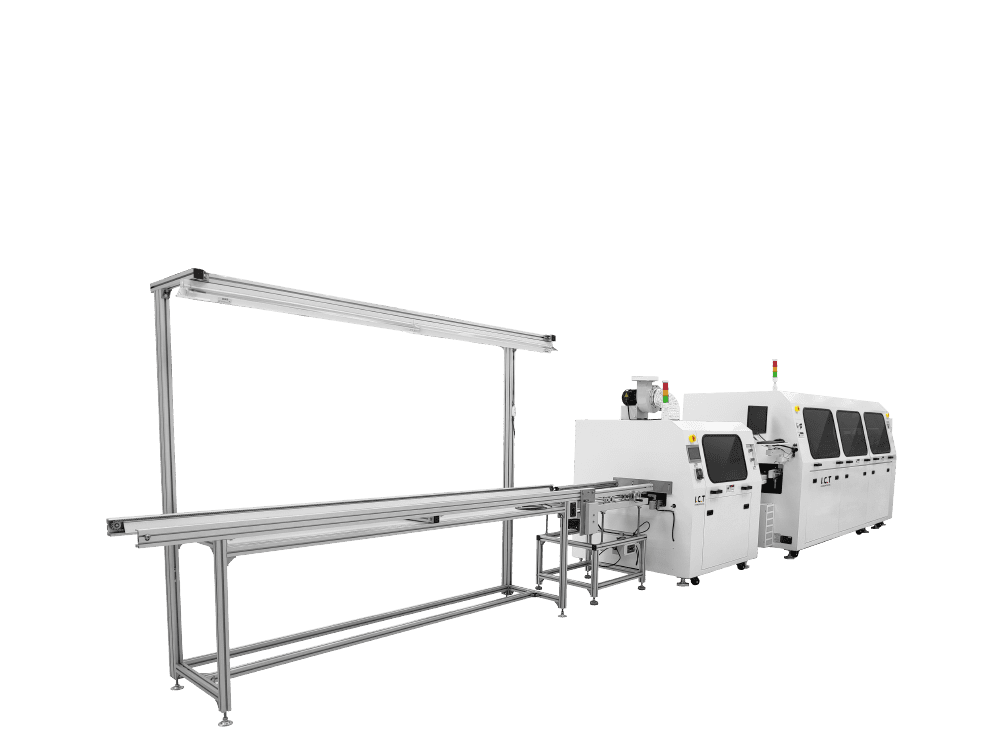
DIP Line Solution
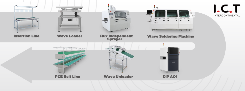
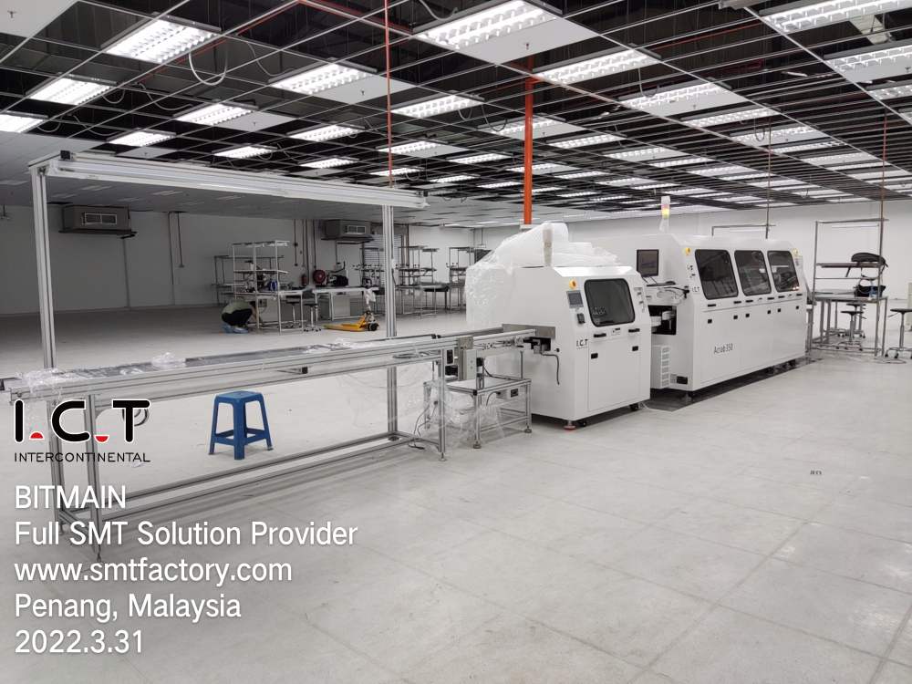
The main DIP equipments are Insertion Line, Wave loader, wave soldering machine, wave unloader and belt assembly line.
What is Dual In-line Package (DIP)?
Dual In-line Package (DIP) is a common form of electronic component packaging. DIP packages are characterized by having a large number of pins arranged in two rows, with the pins spaced and sized to fit into the holes on a printed circuit board for electrical connection.
Initially, DIP packaging was widely used for packaging digital circuit components such as integrated circuits and logic chips. However, as electronic technology has developed, DIP packaging has been widely used for other types of electronic components, such as analog circuit components, memory chips, operational amplifiers, sensors, capacitors, resistors, and more.
DIP is a type of Through-Hole Technology (THT) electronic component packaging. In THT technology, the pins of electronic components pass through holes in the circuit board and are connected to other components on the board through soldering or other methods.
Importance and Features of DIP Line Equipment
Using the example of an entry-level DIP assembly line
Insertion Line
Wave Loader
Wave Soldering Flux Independent Sprayer
Wave Soldering Machine
DIP AOI Machine (after soldering)
Wave Unloder
PCB Belt Line
- Insertion line: used to insert the pins of electronic components into the holes of the circuit board. Plug-in wire equipment includes automatic and semi-automatic plug-in machines, which can be selected according to production scale and requirements.
- Wave loader: the machine used to send the circuit board into the wave soldering process for soldering.
- Wave soldering flux independent sprayer: used to spray a layer of protective agent on the circuit board before soldering the electronic components. The main function of the protective agent is to prevent oxidation and contamination of the circuit board during the soldering process, ensuring the reliability and service life of the circuit board.
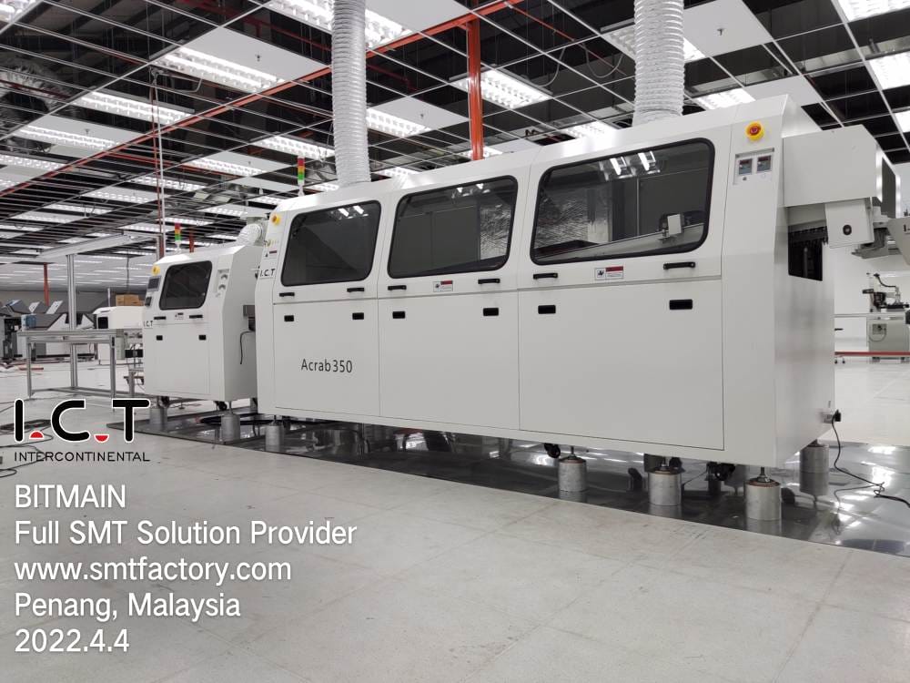
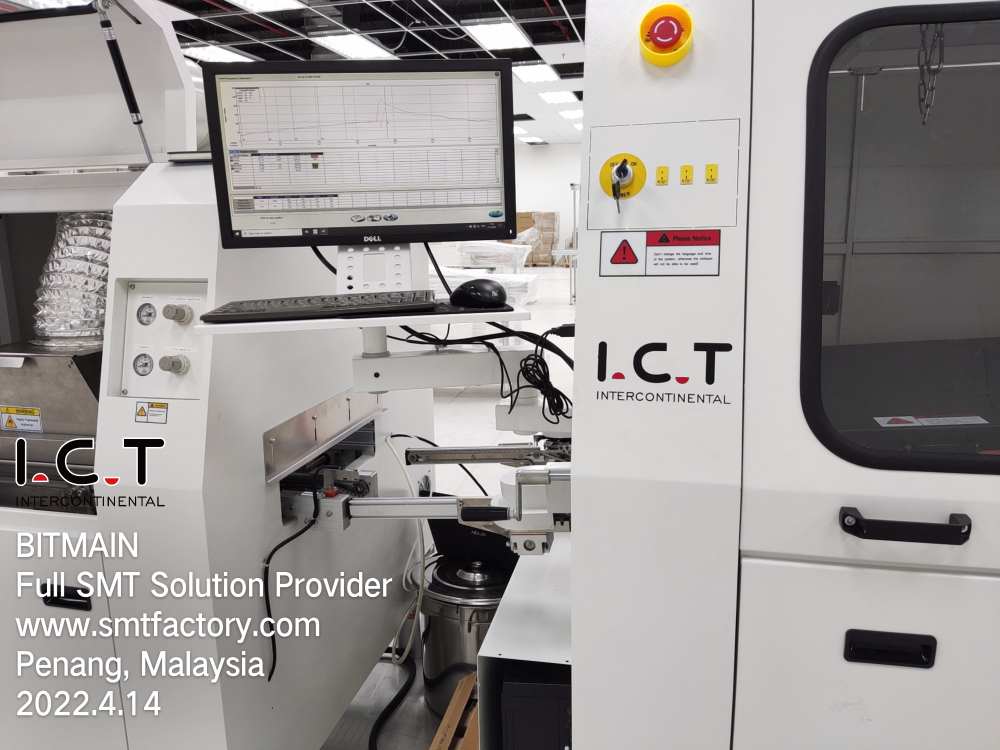
- Wave soldering machine: the Wave Soldering Process of heating the circuit board that has been through the loading machine, melting the solder paste, and attaching it to the pins and pads of the circuit board.
- DIP online inspection AOI (after soldering) : can help quickly detect welding defects such as short circuits, open circuits, offset, missing solder joints, etc., and improve the quality and reliability of the circuit board.
- Wave unloader: automatically sends the completed circuit board out of the wave soldering process and into the next process.
- PCB belt line: used to transport the soldered and tested circuit boards to the subsequent packaging and testing processes. The conveyor belt equipment can be customized according to production requirements, such as selecting different conveying speeds and directions.
In summary, DIP production line equipment plays a crucial role in the production process of DIP packaged components. I.C.T can provide efficient, stable, high-precision, flexible, and customizable equipment to meet the needs of different customers.
DIP Line process
The DIP assembly line process can be divided into 7 steps: component forming and processing, insertion, wave soldering, DIP AOI inspection, component cutting, soldering, cleaning, and functional testing:
- Component forming and processing: Component forming and processing is a critical step in the DIP production process. In this step, DIP components are processed by the manufacturer to specific shapes and sizes.
- Insertion: Insertion is the process of inserting DIP components onto a substrate. In the insertion process, the pins of the component are inserted into the solder pads on the substrate.
- Wave soldering: Wave soldering machine is the process of soldering DIP components to the substrate. In this process, solder paste is applied to the pins and pads, and the solder is melted using a wave soldering machine to secure the component to the substrate.
- DIP AOI inspection: Mainly used for inspecting the soldering quality of the circuit board during the DIP production lineprocess.
- Component cutting: After wave soldering, it is necessary to cut the pins of the DIP component to meet specific size and length requirements.
- Soldering repair (also known as rework): is required for PCBA finished boards that have incomplete solder joints identified during inspection.
- Cleaning: PCB cleaning machines are used to remove residue, dirt, and grease produced during the soldering process from the substrate. This ensures the quality and reliability of the solder joint.
- Functional testing: In the final stage of production, DIP components are subject to functional testing, which typically includes visual inspection, electrical testing, and reliability testing.
Advantages of DIP Line Process
The DIP process, also known as Dual In-line Package process, has the following advantages
- High reliability: The DIP package has a simple structure and reliable solder joints, which results in high reliability. Additionally, DIP packages have fewer pins, which reduces the difficulty and failure rate of circuit board wiring.
- Broad applicability: The DIP package is widely used in various circuit designs, including digital circuits, analog circuits, and power circuits.
- High cost-effectiveness: The manufacturing cost of DIP packaging is relatively low because it does not require complex automation equipment and technology, making it suitable for large-scale production.
- Convenient maintenance: The simple structure of the DIP package makes it easy to maintain and replace without damaging other components.
- Easy connection with external devices: The pins of the DIP package are connected to the circuit board by directly inserting them into the holes on the circuit board, making it easy to connect with external devices.
Application of DIP technology in electronic products
DIP packaged components are widely used in electronic products such as televisions, stereos, computers, communication equipment, security equipment, etc. The advantages of DIP packaging include small size, high reliability, and long service life, which can meet the requirements of different electronic products for component packaging.
What’s the difference between SMT and DIP assembly?
SMT and DIP are two different electronic component assembly technologies, and their main difference lies in the way electronic components are connected.
DIP (Dual In-line Package) is a traditional form of component packaging where the pins are directly inserted into the holes on the circuit board, hence called “through-hole” components. DIP packaging has the advantages of high soldering reliability and low manufacturing cost, but it requires more space, thus it is usually only suitable for simpler circuit designs.
SMT (Surface Mount Technology) is a modern form of component packaging where the pins of the components are directly soldered on the surface of the circuit board instead of being connected through holes. This packaging method allows the components to be arranged more compactly on the circuit board, greatly reducing the volume and weight of the board. In addition, SMT can be produced efficiently through automated assembly lines, therefore SMT gradually replaced DIP as the mainstream electronic component assembly technology.
Advantages of DIP over SMT
- Temperature: The longer pin length of DIP components can better protect the circuit board and components from thermal stress caused by temperature changes in certain special situations, such as high-temperature and high-pressure environments.
- Convenient maintenance: DIP components are typically installed on circuit boards via dual inline packaging, making it easy to maintain and replace components, such as checking the electrical performance of components and replacing faulty ones.
- Safe and reliable: DIP components are generally soldered using through-hole insertion, which is more reliable than the surface mount technology used for SMT components and can work stably in harsh working environments.
- High cost-effectiveness: DIP assembly uses traditional component insertion and wave soldering technology, which is simple to manufacture and has low cost. For applications sensitive to cost, DIP assembly is a more economical choice.
- Wide range of applications: DIP assembly technology is suitable for large, heavy, high-power components, such as some large inductors and transformers.
If there is a need to optimize your SMT line services. Find out how I.C.T’s exclusive line assessment service can improve your operations.
I.C.T Customer`s Case
I.C.T’s partner in Kazakhstan began their collaboration in 2020 when they purchased a fully automated SMT Production Line and a DIP production line from I.C.T for a university in Russia. In 2023, they purchased I.C.T’s fully automated SMT production line and DIP Assembly Line for their new factory in Kazakhstan to produce security cameras and other product
