Advantages of 3D Measurement in Solder Paste Inspection Systems
In the past, Solder Paste Inspection (SPI) systems were given lower priority compared to Automated Optical Inspection (AOI) systems for solder joints. While AOI systems detect defects at the end of the production line, inspecting solder paste immediately after application significantly improves the production process. Although final product inspection remains essential, the primary goal of any manufacturer is to produce a high-quality product without incurring repair costs. To achieve this, it is crucial to monitor and manage each stage of the production process. Poor solder paste application is often the root cause of defects that manifest later in the production process. Figure illustrates the formation of the “tombstone” defect, where the soldering process reveals a defect, but it is not the cause of it.

The Advantages of 3D Measurement in Solder Paste Inspection
Is Selective Solder Paste Inspection Enough?
Today, some production lines include a printer with built-in 2D solder paste inspection and an independent SPI system. However, to maintain the printer’s speed, the built-in inspection system only checks a few sections of solder paste application, while the independent inspection only performs selective checks, which cannot guarantee defect-free boards.
Only full-surface inspection can detect random defects, and only inspection of the entire series (every board) can identify deviations in printer performance. For example, a trend of decreasing solder paste volume across the series may indicate aperture contamination.
The Impact of Aperture Size on Print Efficiency
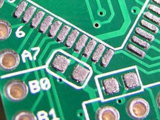
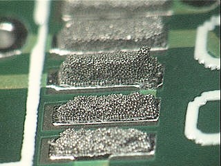
As electronic assemblies shrink and component density increases, stencil aperture sizes decrease, and their number continues to grow. Different stencil aperture sizes affect the transfer efficiency, where smaller apertures result in less solder paste being transferred to the PCB.
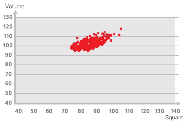
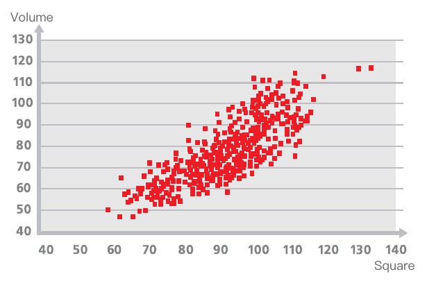
Comparing two round stencil apertures with diameters of 700 µm and 270 µm at the same stencil thickness of 100 µm, we can evaluate the print efficiency. In Figure 2a, the print area for the 700 µm aperture shows that the application area varies from 75% to 100%, with a volume above 90%, which is a satisfactory result. However, for the 270 µm aperture, the application area ranges from 60% to 120%, and the volume from 50% to 100%. This indicates that quality control of solder paste application on small apertures becomes a critical factor for ensuring solder joint quality.
2D or 3D Inspection?
SPI suppliers offer both 2D and 3D systems for solder paste inspection. 2D inspection relies on comparing different shades of gray, requiring extensive setup depending on the PCB color, and lacks precise volume information.
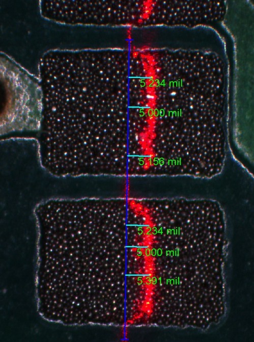
3D systems measure the height of the PCB and solder paste. Today’s 3D inspection systems use two technologies: laser measurement and multi-frequency moiré. Laser measurement detects many defects that may be missed in traditional 2D inspection but has limitations, such as being unable to measure the volume of a specified area, inaccuracies due to the large laser beam thickness, and sensitivity to PCB color.
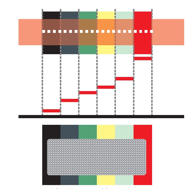
Multi-frequency moiré measures the height of each pixel on the inspected object’s surface. Light is projected onto the object from multiple angles (4 or 8, depending on the system), creating lines reminiscent of a diffraction grating. Any irregularity or relief on the surface causes the projected lines to shift, allowing height measurement at each point with an accuracy of up to 1 µm. Knowing the height and area of the inspection object allows for the calculation of its volume. Unlike classic systems, 3D measurement with multi-frequency moiré provides precise volume measurements in numerical terms.
The I.C.T-S400 3D SPI System
The new generation of the I.C.T-S400 series represents high-precision and high-performance SPI systems. The latest model, I.C.T-S400, offers three times the inspection speed without sacrificing performance or accuracy. Utilizing a patented dual-light projection, the system eliminates the “shadow effect” common in most 3D SPI systems. Additionally, the I.C.T-S400 resolves PCB deformation issues, which significantly impact inspection accuracy and reliability.
The new, user-friendly graphical interface with a touchscreen maximizes operator convenience. The optimized menu and revolutionary new interface make operation easier and more straightforward. The 3D view allows operators to instantly evaluate test results. The I.C.T-S400 requires no extensive programming or debugging.
