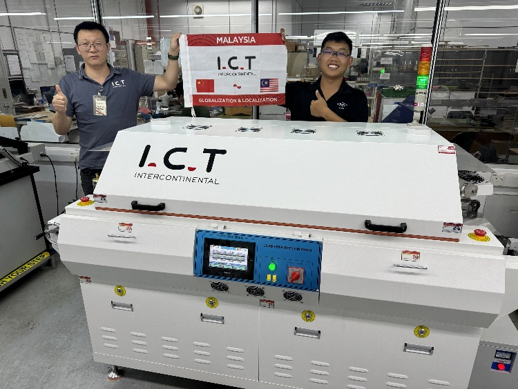
Reflow Soldering Challenges in Power Electronics PCB: How to Improve Thermal Stability and Yield

Reflow soldering in power electronics PCB assembly is much more demanding than in ordinary consumer electronics. Engineers often face high thermal mass, large copper pours, thick boards, heavy components, and tighter reliability expectations, while factory managers also need to control defect rates, throughput, and operating cost at the same time. In practice, many of these problems cannot be solved by changing one temperature setting alone. They usually require the right advanced reflow oven solutions, better profile design, stronger board support, and a more stable process window. This article explains the key reflow soldering challenges in power electronics PCB manufacturing and how to improve thermal consistency, solder joint quality, and production yield.
Table of Contents
- 1. Why Power Electronics PCBs Are More Difficult to Reflow
- 2. Uneven Thermal Mass and Heat Distribution Problems
- 3. Thick Boards, Heavy Copper, and Profile Design Challenges
- 4. Voiding, Wetting, and Reliability Risks in Power Electronics PCBA
- 5. PCB Warpage and Mechanical Stability During Reflow
- 6. Process Strategies to Reduce Defects and Improve Yield
- 7. How to Choose the Right Reflow Oven for Power Electronics PCB Production
- 8. How I.C.T Helps Stabilize Reflow in Power Electronics Manufacturing
- 9. FAQ
1. Why Power Electronics PCBs Are More Difficult to Reflow
Power electronics assemblies often include large copper planes, thick substrates, high-current paths, heat-spreading structures, and components that behave very differently from standard SMT consumer boards. That means the reflow window is usually narrower, and the cost of thermal mismatch is much higher.
Thermal behavior is less uniform across the same board
On a power electronics PCB, some zones absorb heat very slowly while others rise in temperature much faster. This makes it difficult to maintain a balanced profile across the whole assembly. If the profile is too weak, solder may not wet properly in heavy-mass areas. If it is too aggressive, lighter areas may overheat.
Reliability expectations are usually higher
Many power electronics products are used in industrial control, energy systems, automotive electronics, and other demanding applications. In those environments, reflow quality affects not only initial yield, but also long-term thermal cycling performance, solder fatigue resistance, and field reliability.
Process mistakes become more expensive
Because power boards often use higher-value components and stricter acceptance requirements, a reflow defect can create much more cost than in an ordinary SMT product. That is why process stability matters far more than one-time success.
2. Uneven Thermal Mass and Heat Distribution Problems
One of the most common reflow challenges in power electronics PCB manufacturing is uneven heat absorption. Large copper pours, thermal pads, metal-core sections, and mixed component sizes all make heat distribution harder to control.
Large copper areas absorb heat slowly
Boards designed for current handling and heat dissipation usually contain heavy copper or large thermal regions. These areas delay solder melting and can create insufficient wetting if the profile is not properly matched to the board structure.
Mixed component density complicates profile balance
A single board may include large power devices, connectors, transformers, and smaller signal components at the same time. This mixed layout makes it difficult to set one profile that protects smaller parts while still delivering enough energy to larger thermal-mass zones.
In many cases, manufacturers need a profile strategy closer to thick PCB reflow profile design than a standard SMT recipe, because the thermal response of the assembly is fundamentally different.
Hot spots and cold spots affect solder consistency
When the board does not heat evenly, some solder joints may reflow too early while others lag behind. This creates inconsistent joint formation, unstable wetting behavior, and more difficulty achieving repeatable process control from batch to batch.
3. Thick Boards, Heavy Copper, and Profile Design Challenges
Profile design for power electronics PCB assembly should not be treated as a routine setup task. The thicker the board and the heavier the copper structure, the more carefully the heating curve must be built.
Soak and ramp settings need tighter control
If the ramp-up is too fast, thermal stress may rise sharply across different board regions. If the soak stage is too weak, larger thermal-mass areas may still not be ready when the peak zone arrives. If the total thermal input is too strong, oxidation, component stress, or resin damage can become more likely.
Peak temperature alone is not enough
Many factories focus too much on peak temperature, but for power boards the more important question is whether the whole assembly spends enough time in the proper melting window. Time above liquidus, thermal balance, and cooling slope all matter.
Board construction changes the ideal recipe
FR-4 thickness, copper weight, thermal pad size, solder paste volume, and underside copper distribution all influence the final profile. This is one reason reflow recipes from ordinary products rarely transfer directly to power electronics boards without adjustment.
4. Voiding, Wetting, and Reliability Risks in Power Electronics PCBA
Power electronics assemblies often use packages and pad structures that are especially sensitive to reflow quality. Poor thermal control does not just create visual defects. It can directly reduce electrical and thermal reliability.
Voiding becomes a bigger concern in thermal pads
Power devices often rely on thermal pads for heat transfer. If the reflow process causes excessive voiding, thermal resistance may increase and long-term device performance can suffer. That makes process optimization especially important for heat-sensitive applications.
Insufficient wetting can hide deeper process imbalance
When heavy-mass zones do not receive enough heat, the result may be weak wetting, partial collapse, or unstable solder fillets. These problems are often symptoms of poor thermal distribution rather than simple operator error.
Defect prevention must be linked to board type
Some of the same control logic also appears in other reliability-focused sectors. For example, manufacturers working to reduce common reflow soldering defects in automotive PCBA often face similar challenges around temperature stability, joint quality, and process discipline.
5. PCB Warpage and Mechanical Stability During Reflow
Warpage is another major challenge in power electronics PCB assembly. When thermal expansion is uneven, the board can deform during heating and cooling, affecting solder joint formation and placement stability.
Heavy structures increase bending risk
Thicker boards and large copper imbalance can amplify mechanical stress during reflow. This is especially important when the board contains large thermal pads, asymmetric copper distribution, or heavy top-side components.
Warpage affects solder joint alignment
If the board bends during reflow, solder joints may experience uneven collapse, coplanarity issues, or stress concentration. This is one reason mechanical support and profile design should be considered together, not separately.

Prevention requires both design and process control
Factories dealing with these issues often need to review support tooling, conveyor setup, profile shape, and board design together. That is also why guidance on how to avoid warpage in multi-layer PCB reflow remains highly relevant for power electronics production.
6. Process Strategies to Reduce Defects and Improve Yield
Improving yield in power electronics PCB reflow is not about chasing one perfect number. It requires repeatable process discipline across materials, profiling, equipment setup, and inspection.
Profile around the actual board, not the standard recipe
Each power board should be evaluated based on its real thermal response, not just a template profile used for ordinary assemblies. Thermocouple placement, board mapping, and repeated validation matter more here than in simpler products.
Stabilize materials and oven loading conditions
Solder paste behavior, board loading, conveyor consistency, and thermal environment should remain as stable as possible. If loading changes frequently, profile repeatability can drift and make troubleshooting harder.
Control energy use without sacrificing process window
Factories often want to reduce energy cost, but aggressive energy saving can narrow the process window if it weakens thermal stability. That is why process review should include both yield and reflow oven energy consumption cost considerations, instead of optimizing one side alone.
7. How to Choose the Right Reflow Oven for Power Electronics PCB Production
The right oven for power electronics assembly should support stable thermal transfer, sufficient heating capability, repeatable conveyor behavior, and practical control over different board types.
Zone structure and thermal capacity matter
When boards have larger thermal mass, the oven must provide enough control flexibility and heating reserve. In many lines, an 8-zone reflow oven or a stronger configuration can give a more stable process window than a lighter setup.
Nitrogen capability can support higher process consistency
For some products, nitrogen reflow can help reduce oxidation and improve wetting consistency, especially where joint quality expectations are strict. Manufacturers evaluating a lead-free nitrogen reflow oven should look at actual process needs, not just equipment specifications.

Equipment selection should still be process-driven
The best answer is not always the oven with the largest number of features. The right choice depends on the board mix, thermal mass, throughput target, process tolerance, and future production plan. In many cases, this is where manufacturers return to broader reflow oven solution planning instead of evaluating hardware in isolation.
8. How I.C.T Helps Stabilize Reflow in Power Electronics Manufacturing
At I.C.T, we do not treat reflow soldering as a stand-alone oven setting issue. We look at the whole production condition: board structure, thermal demand, product reliability target, and line configuration.
We match equipment choice to real board behavior
Power electronics boards often require a stronger combination of profile engineering, oven capability, support strategy, and validation method. That is why equipment recommendation should be based on actual assembly conditions instead of generic machine comparison.
We focus on stable production, not one-time profile success
Our goal is not just to help a factory pass one trial. It is to help them keep thermal balance, reduce defect risk, and improve repeatability under real mass-production conditions.
Better process control leads to better yield and lower hidden cost
Once reflow is stabilized, factories usually gain more than just fewer solder defects. They also reduce rework, scrap, process drift, and unnecessary energy waste, which creates a stronger overall return.
Need a More Stable Reflow Process for Power Electronics PCB Assembly?
I.C.T helps manufacturers evaluate board thermal behavior, optimize reflow profiles, choose suitable oven configurations, and improve mass-production stability for demanding electronics applications.
9. FAQ
Why is reflow soldering more difficult for power electronics PCB assemblies?
Because power electronics boards often have larger copper areas, thicker substrates, heavier components, and stricter reliability targets. These factors make thermal balance and solder consistency harder to control during reflow.
What is the biggest thermal challenge in power electronics PCB reflow?
The biggest challenge is usually uneven thermal mass. Some board areas heat much more slowly than others, so the process window becomes narrower and more sensitive to profile design errors.
Why is voiding important in power electronics solder joints?
Because excessive voiding can reduce thermal transfer efficiency under power devices, which may affect temperature control, long-term reliability, and real operating performance.
Can one standard reflow profile work for all power electronics boards?
Usually not. Power electronics boards differ widely in thermal mass, copper layout, thickness, and component mix, so profile settings normally need to be matched to the actual assembly design.
How can manufacturers improve reflow yield in power electronics PCB production?
They should combine profile validation, stable materials, proper board support, suitable oven capability, and continuous process review instead of relying on one recipe change alone.